Powering The Future: The Role Of Patterned Wafers In Solar Cell Technology
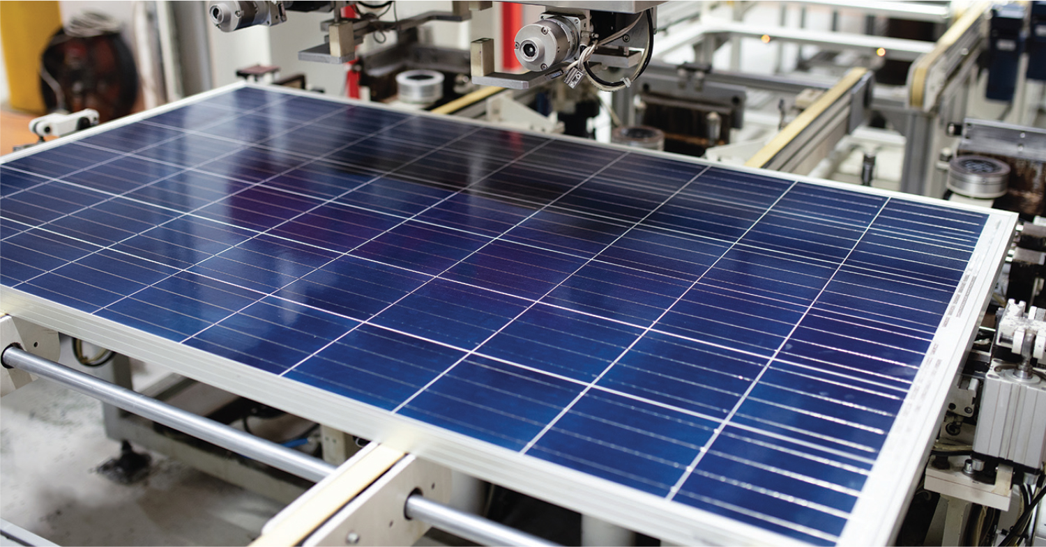
The solar wafer is a tiny piece of silicon crystals that serves as a basis for small-scale gadgets to create semiconductors for sun cell production. Directly converting solar energy into electricity via the photovoltaic energy production system depends heavily on this wafer. The wafers are given an uneven texture to boost their efficiency for manufacturing solar cells after cleansing the particles.
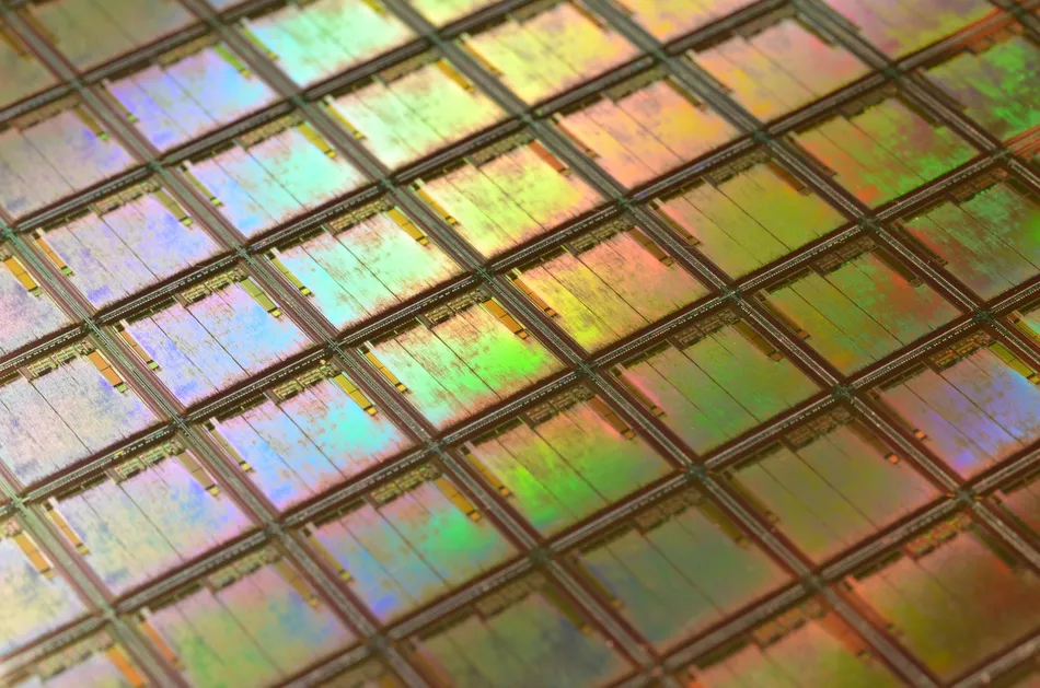
The technique of photolithography helps in creating Patterned Wafers. Finding fatal flaws in factory-made wafers requires patterned wafer inspection. In the current technological era, they are essential for everything from computing devices and solar cells to nanotechnology and medicinal sensors. Due to its numerous benefits over conventional unpatterned ones, patterned silicon wafers are increasingly prevalent in the semiconductor sector. These benefits include better homogeneity, higher dependability, and lower unpredictability.
Process Of Making Patterned Wafers
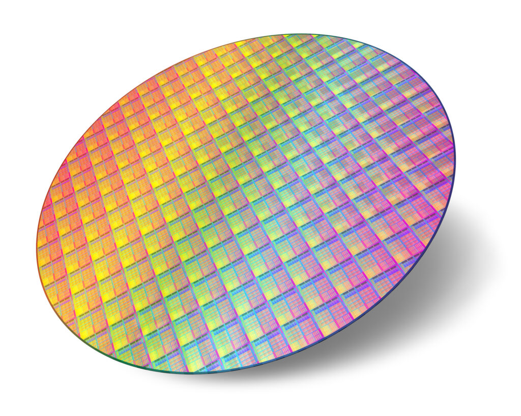
The process of creating patterned wafers involves the technique of photolithography. It entails transferring patterns onto the wafer with light to create patterns on the surface of the wafer. This procedure is often done in a clean room to avoid polluting the wafer with dust or other particles.
A polished silicon wafer, a tiny portion cut from polycrystalline or monocrystalline slabs of pure silicon, is the basis for the entire process. After that, this disc goes through multiple processes to prepare it for patterning. Initially, a photosensitive substance is put onto the wafer. It is pre-marking where notches can go and which portions will remain unperturbed when exposed to specific agents. It acts to safeguard any areas that require to stay intact during etching. Concerning the use of the photolithography method, the photoresist can be either negative or positive.
You now transfer the pattern to the wafer using a UV light source. The UV light may occasionally be unable to reach certain areas of the wafer by a specific mask. On exposure to UV light, the photosensitive substance undergoes a chemical reaction creating a pattern on the wafer. It is essential to eliminate any residual photosensitive substance on the wafer in forming the pattern.
After that, either heat or a specific chemical solvent is used. On each square millimeter of the wafer, hundreds, thousands, or even millions of particular features could be printed once it is finished.
When creating a pattern, a base layer of silicon that has typically been oxidized is coated with a photoresist and is visible to light using an image mask. Each layer is etched by its design parameters after multiple repetitions of this process. Many businesses outsource their patterning requirements instead of trying it themselves because the process calls for extreme precision and skill.
Uses Of Patterned Wafers
Given the numerous benefits over conventional silicon ones, patterned wafers are rising and becoming prominent as a technology. Consumer electronics to large-scale industries both benefit from utilizing these cutting-edge wafers. Here are a few of the many typical applications for patterned chips:
- Using patterned wafers, you can make capacitors, transistors, resistors, and other parts like computer processors and electronic circuits (ICs).
- The photovoltaic systems on satellites and other spaceships can also use these wafers as solar cells.
- Small healthcare equipment that requires precision monitoring of electrical impulses within their circuitry, such as pacemakers or hearing aids, benefit significantly from developing patterned silicon wafers.
- The complex sensors and chipsets developed utilizing patterned silicon technology are a significant component of increasingly automated vehicles. These elements are essential to modern vehicle engineering, from driverless car navigation systems to cutting-edge safety measures like lane departure warnings.
- Because it can accurately gauge changes in voltage across various spots on the chip surface, patterned technology is feasible for sensors to have higher sensitivity than ever before. Therefore they are perfect for measuring pressure, humidity, and temperature.
Benefits Of Utilizing Patterned Wafers In Solar Cell Technology
Numerous benefits of patterned silicon chips are revolutionizing the semiconductor manufacturing industry. These advantages are:
1. Cost Effective
By cutting out procedures or materials that aren’t necessary, manufacturers can produce wafers at a lower cost by using patterning techniques like photolithography.
2. Uniform And Reliable
The surface patterns produce homogeneity throughout each chip, enhancing dependability for testing and application in many products. Additionally, it can build incredibly intricate structures without sacrificing their electrical or structural stability.
3. Better Performance
The surface is etched to provide microscopic channels that improve heat absorption. Furthermore, its accuracy enhances device performance, making it perfect for radio frequency transceivers and microprocessors, among other devices.
4. Easy And Flexible
Thanks to patterning methods, engineers have far more freedom when creating innovative components or gadgets. Patterned wafers can rapidly test several designs without going through a whole fabrication cycle since they can modify factors like feature size, line widths, spacing between lines, etc.
Significance Of Patterned Wafers In Powering The Future

Patterned wafers are necessary to create the microprocessor chips that go into electronic gadgets. The requirement for more complex patterned wafers is growing due to the development of new technologies, including quantum information processing, 5G connectivity, and the World Wide Web.
These patterned chips must be produced using extraordinarily accurate and precise manufacturing techniques and materials distinct from conventional chips. The importance of patterned wafers in determining the course of the electronics industry will increase as these new technologies continue to advance. Although these wafers are essential for contemporary technology as raw materials, patterned wafers open up even more opportunities for engineering uses.
Conclusion
Numerous sectors have undergone revolutions through the use of patterned silicon wafers. It is because of its capacity to produce complex patterns at a microscopic scale accurately. Such technology will create new opportunities in various industries, including consumer electronics, robotics, aerospace engineering, healthcare, etc. These emerging technologies are significant because they will allow manufacturers’ fastest-ever production of tiny chips.
Businesses and customers may choose their technology and supplies wisely if they are aware of how patterned silicon wafers are made and the uses and benefits they provide. Patterned silicon wafers will undoubtedly be a key component of technology in the future owing to their superior efficiency, better flexibility, and lower price.